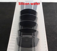
Silicon (Si) Wafers Product
Specifications:

Growth method : CZ/FZ
Diameter : 2’’/3’’/4’’/6’’/8’’/10’’/12’’
Thickness   : 275-775µm
Orientation : <100>, <111> & <110>
Conductivity : P-type / N-type / Intrinsic
Resistivity : 0.001-10000 Ohm-cm
Dopant : Boron / Phosphorous / Antimony / Arsenic
Surface : One side polished (SSP) / Double sides polished (DSP)
Grade : Prime/Test/Dummy/Mechanical

Request for Quote
Thermal Oxide (SiO2) Wafers Product
Specifications:

Oxidation Technique : Wet Oxidation or Dry Oxidation
Diameter: 2’’/3’’/4’’/6’’/8’’/10’’/12’’
Oxide Thickness: 100-500 Å
Tolerance: +/-5%
Surface: One side or double side oxide layers

Request for Quote
Silicon On Insulator (SOI) Wafers SOI
Handle Substrate

Growth method : CZ/FZ
Diameter : 3’’/4’’/6’’/8’’
Orientation : <100>, <111> & <110>
Conductivity : P – type / N – type / Intrinsic
Resistivity : 0.001-10000 Ohm-cm
Dopant : Boron / Phosphorous / Antimony / Arsenic
Back Surface : Etched or Polished with/without oxide
Handle wafer : >=300 µm

Specifications:
Device Layer

Growth method : CZ/FZ
Diameter : 3’’/4’’/6’’/8’’
Device Thickness : 0.5-300 µm
Orientation : <100>, <111> & <110>
Conductivity : P – type / N – type / intrinsic
Resistivity  : 0.001-10000 Ohm-cm
Dopant : Boron / Phosphorous / Antimony / Arsenic
Front Surface : Polished
Surface Roughness : ≤ 0.4nm

Buried Oxide (BOX) Layer

Oxide Thickness : 500 Å-6 µm
Tolerance : +/-5%

Request for Quote
Sapphire Wafers Product
Specifications:

Diameter : 2’’/4’’/6’’
Thickness : 0.43 mm / 0.50 mm / 1 mm
Orientation : <0001>=C-plane / <1120> =A-plane <1102> =R-plane & <1010>=M-plane
Surface  : One side polished (SSP) / two sides epi polished (DSP)
Roughness : Ra ≤ 5 Å

Request for Quote
Indium Phosphide (InP) Wafers Product
Specifications:

Growth method : LEC/VGF
Diameter : 2’’/3’’/4’’
Thickness : 350-625 µm
Orientation : <100>, <111> & <110>
Conductivity : P – type / N – type / Semi-conducting/Semi-insulating
Concentration : 1E8-8E18 cm-3
Dopant : S / Z / Fe / Undoped
Surface : One side polished (SSP) / Double sides polished (DSP)

Request for Quote
Gallium Nitride (GaN) Epitaxial Wafers
P-GaN/N-GaN on Sapphire Specifications:

Growth method : MOCVD/HVPE
Conductivity : P-type/N+-type
Dopant : Mg/Si
GaN Thickness : 1-5 µm / 500nm-100 µm
Concentration : >5E17 cm-3 / >1E18 cm-3
Resistivity : < 0.05 Ohm-cm
Surface : One side polished (SSP) / Double sides polished (DSP)
Substrate Diameter : 2’’/3’’/4’’ Sapphire wafer

Request for Quote
Indium Tin Oxide (ITO) Coated Glass

Length (L) × Width (W) × Thickness : 50 mm × 50 mm × 0.7mm/1.1 mm/2.2mm Length (L) × Width (W) × Thickness : 175 mm × 175 mm × 0.7mm/1.1 mm/2.2mm Surface Resistivity : 10 ohms/sq & 15 ohms/sq
Transmittance : :≥85%

Any others size can be arranged on customer demand.
Request for Quote
Fluorine doped Tin Oxide (FTO) glass

Length (L) × Width (W) × Thickness : 50 mm × 50 mm × 0.7mm/1.1 mm/2.2mm Length (L) × Width (W) × Thickness : 175 mm × 175 mm × 0.7mm/1.1 mm/2.2mm Surface Resistivity  : 10 ohms/sq & 15 ohms/sq & above
Transmittance : ≥85%

Any others size can be arranged on customer demand.
Request for Quote
Quartz & Glass Plates

Length (L) × Width (W) × Thickness : 10 mm × 10 mm × 1 /2/3/4/5 mm Length (L) × Width (W) × Thickness : 25 mm × 25 mm × 1 /2/3/4/5 mm Length (L) ×
Width (W) × Thickness : 50 mm × 50 mm × 1 /2/3/4/5 mm Length (L) ×
Width (W) × Thickness : 75 mm × 25 mm × 1 /2/3/4/5 mm Length (L) ×
Width (W) × Thickness  : 75 mm × 75 mm × 1 /2/3/4/5 mm Length (L) ×
Width (W) × Thickness : 100 mm × 10 mm × 1/2/3/4/5 mm

Any others size can be arranged on customer demand.
Request for Quote
99.7% Alumina Subtrate

Length (L) × Width (W) × Thickness : 8 mm × 8 mm × 0.5 mm
Length (L) × Width (W) × Thickness : 8 mm × 8 mm × 1 mm
Length (L) × Width (W) × Thickness : 10 mm × 10 mm × 0.5 mm
Length (L) × Width (W) × Thickness : 10 mm × 10 mm × 1 mm
Length (L) × Width (W) × Thickness : 20 mm × 20 mm × 0.5 mm
Length (L) × Width (W) × Thickness : 20 mm × 20 mm × 1 mm
Length (L) × Width (W) × Thickness : 25 mm × 25 mm × 0.5 mm
Length (L) × Width (W) × Thickness : 25 mm × 25 mm × 1 mm

Any others size can be arranged on customer demand.
Request for Quote
96% Alumina Substrate 19 x 19 mm with Laser Striation

Length (L) × Width (W) × Thickness : 19 mm × 19 mm × 0.65 mm

Any others size can be arranged on customer demand.
Request for Quote
Any others substrates/wafers can be arranged on customer demand.